


All Products
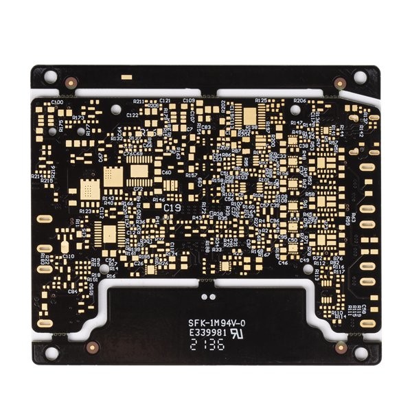
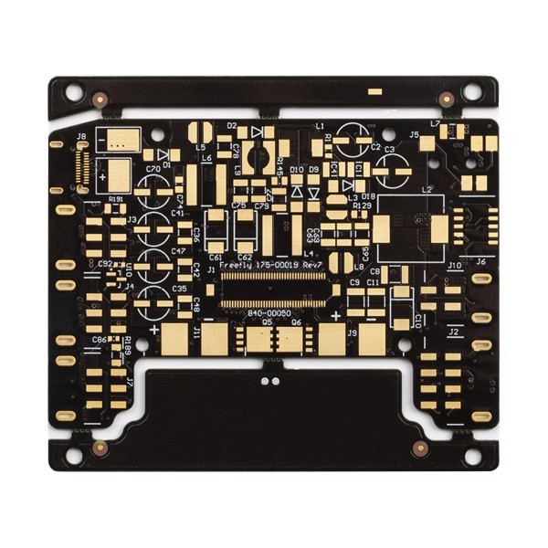
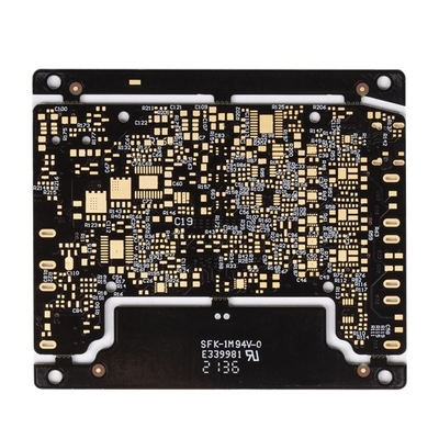
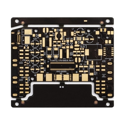
1.2mm 8 Layer HDI PCB Board fabrication

Contact me for free samples and coupons.
Whatsapp:0086 18588475571
Wechat: 0086 18588475571
Skype: sales10@aixton.com
If you have any concern, we provide 24-hour online help.
xProduct Details
| PCB Name | 8L 3+N+3 HDI Boards | Marterial | FR-4, TG170 |
|---|---|---|---|
| Board Layer | 8L | Board Thickness | 1.2mm |
| Copper Thickness | 2/1/1/1/1/1/1/2oz Finished | Min.PCB Track/gap | 4/6mil |
| Solder Mask | Black Color KSM | Smallest Mechanical Drilling Hole | 0.25mm |
| Special Request | Buried Vias And Blind Vias, Three Step Stack Up | Application | Industrial Control |
| Highlight | 1.2mm HDI PCB Board,ODM HDI PCB Board,1.2mm high density circuit board |
||
Product Description
1.2mm 8 Layer HDI PCB Board
HDI PCB Board PCB Board Assembly PCB And PCBA 8 Layer PCB Quick PCB Prototype Low Volume PCB High Frequency PCB
8L 3+N+3 HDI Boards
What’s HDI PCB? High-density interconnect (HDI) PCBs are characterized by finer lines, closer spaces, and more dense wiring, which allow for a faster connection while reducing the size and bulk of a project. These boards also feature blind and buried vias, laser ablated microvias, sequential lamination, and via in-pads.
As a result, a HDI board can house the functionality of the previous boards used. MADPCB is an HDI PCB manufacturer and provider in Shenzhen, China supports HDI PCB prototype and mass production with less expensive price and quick-turn lead time. Customers from a variety of industries we serve have a common that have high expectations in quality, reliability and on-time delivery in HDI PCB production. Our quality is not afterthought, but built into each process from front-end to fabrication and shipping.
| Layer counts: | 8 layer | Circuit board laminate: | FR4 TG170 S1000-2 |
| Different Copper thickness: | 2/1/1/1/1/1/1/2OZ | PCB Board thick: | 1.2 MM |
| Smallest Mechanical drilling hole: | 0.25 mm | Min. line distance/space: | 4/6mil |
| Solder mask color: | Black color KSM | Legends' color: | White color |
| PCB surface finished: | Immersion Gold | Board profile: | Milling |
| PCB Board Application: | industrial control | ||
| Requesting Special requirement: | HDI Buried vias and blind vias, three step stack up /impedance control/resin filled and plated over | ||
![]()
![]()
FAQ:
Q1:Are you a factory or trade company?
A: Yes, we are the factory, we have independent quick turn prototype PCB manufacturing & big volume PCB production lines.
Q2:What kind of PCB file format can you accept for production?
A: Gerber, PROTEL 99SE, PROTEL DXP, POWER PCB, CAM350, ODB+(.TGZ)
Q3:Are my PCB files safe when I submit them to you for manufacturing?
A: We respect customer's copyright and will never manufacture PCB for someone else with your files unless we receive written permission from your side, nor we'll share these files with any other 3rd parties. And we could sign NDA with client if necessary.
Q4:If we have no PCB file/Gerber file, only have the PCB sample,can you produce it for me?
A: Yes,we could help you to clone the PCB. Just send the sample PCB to us, we could clone the PCB design and work out it.
Q5:What is your standard lead time for PCB?
A: Sample/prototype(less than 3sqm):
1-2 Layers: 3 to 5working days (fastest 24hours for quick turn services)
4-8 Layers: 7~12 working days (fastest 48hours for quick turn services)
Mass production (less than 200sqm):
1-2 Layers:7 to 12 working days
4-8 Layers:10 to 15 working days
Q6:What payment do you accept ?
A: Wire Transfer(T/T) or Letter of Credit(L/C) or Paypal(only for small value less than 500usd)
Recommended Products