


All Products
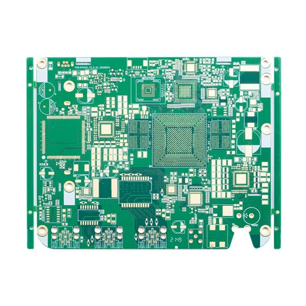
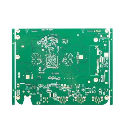
FR4 TG170 HDI PCB Board


Contact me for free samples and coupons.
Whatsapp:0086 18588475571
Wechat: 0086 18588475571
Skype: sales10@aixton.com
If you have any concern, we provide 24-hour online help.
xProduct Details
| PCB Name | 6L 2+N+2 HDI Printed Circuit Board | Marterial | FR4 TG170 |
|---|---|---|---|
| Surface Finished | Immersion Gold | Board Thickness | 2.0mm |
| Copper Thickness | 1/1/1/1/1/1OZ | Min.PCB Track/gap | 3/3mil |
| Solder Mask | Green, Two Sides | Smallest Mechanical Drilling Hole | 0.2mm |
| Special Requirement | HDI Buried Vias And Blind Vias, Two Step Stack Up /0.25mm BGA | Applicationcommunications Products | Industrial Control |
| Highlight | FR4 TG170 HDI PCB Board,TG170 HDI PCB Board,TG170 hdi pcb prototype |
||
Product Description
FR4 TG170 HDI PCB Board
HDI PCB Board HDI Blind Buried Vias Two Step Stack Up PCB Assembly Services Green PCB Board High Density Printed Circuit
6L 2+N+2 HDI Printed Circuit Board
HDI stands for High-Density Interconnector. It is a special type of PCB that has the capability of high-density interconnections. It means that HDI boards has more wires or conduction lines per unit area, utilizing the most out of the space and offering a compact PCB.
HDI PCB has tightly packed interconnections, it saves a lot of space and offers more component density and it has the capability of making a circuit compact.
HDI boards are particularly attractive to portable, mobile, and portable electronics due to their slim, dependable performance and tiny size. HDI technology is a critical component of many of advanced technologies. The miniaturization of electronic components including PCBs has enabled manufacturers to produce smaller, more cost-effective devices without sacrificing performance or reliability.
They are largely used in Consumer Electronics, communication, Automotive and Aerospace,Medical Devices, and industry control products and other industries.
| Circuit board Layer count: | 6L | Circuit board laminate: | FR4 TG170 |
| Layer Copper thick: | 1/1/1/1/1/1OZ | Board thickness: | 2.0MM |
| Smallest hole size: | 0.20mm | Smallest PCB track/gap: | 3/3mil |
| Solder mask color: | Green | Silk screen color: | White |
| PCB surface finished: | Immersion Gold | Board profile: | Routing |
| PCB Board Application: | industrial control | ||
| Requesting Special requirement: | small line space and gap:3/3mil/HDI Buried vias and blind vias, two step stack up /impedance control/0.25mm BGA | ||
![]()
![]()
FAQ:
Q1:Could you provide PCB Assembly services and components sourcing?
A: Yes, we could also provide components sourcing and PCB Assembly services as well as box build if request.
Q2:Which countries have you worked with?
A:USA, Canada, Italy, Germany, UK, Spain, France, Russia, Iran, Turkey, Czech Republic,Austria, Australia, Brazil, Japan, India etc.
Q3:Are my PCB files safe when I submit them to you for manufacturing?
A: We respect customer's copyright and will never manufacture PCB for someone else with your files unless we receive written permission from your side, nor we'll share these files with any other 3rd parties. And we could sign NDA with client if necessary.
Q4:If we have no PCB file/Gerber file, only have the PCB sample,can you produce it for me?
A: Yes,we could help you to clone the PCB. Just send the sample PCB to us, we could clone the PCB design and work out it.
Q5:What is your standard lead time for PCB?
A: Sample/prototype(less than 3sqm):
1-2 Layers: 3 to 5working days (fastest 24hours for quick turn services)
4-8 Layers: 7~12 working days (fastest 48hours for quick turn services)
Mass production (less than 200sqm):
1-2 Layers:7 to 12 working days
4-8 Layers:10 to 15 working days
Recommended Products