


All Products
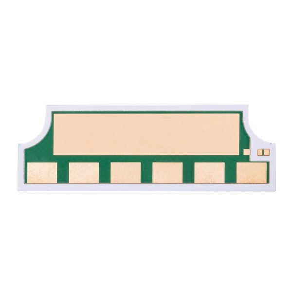
High TG FR4 Ceramic PCB Board


Contact me for free samples and coupons.
Whatsapp:0086 18588475571
Wechat: 0086 18588475571
Skype: sales10@aixton.com
If you have any concern, we provide 24-hour online help.
xProduct Details
| PCB Name | Green Ceramic Base Circuit | Marterial | FR-4;High TG FR4; Ceramic Base Material |
|---|---|---|---|
| Surface Finished | Immersion Gold, LF-HASL, OSP... | Board Thickness | 0.4mm-4.0mm |
| Copper Thickness | 18um-105um | Solder Mask | Green;blue;black;red... |
| Highlight | TG FR4 Ceramic PCB Board,ODM Ceramic PCB Board,TG FR4 Ceramic PCB |
||
Product Description
High TG FR4 Ceramic PCB Board
Ceramic PCB Board Green Ceramic Base PCB Ceramic Base Material High TG Material High Density PCB
Green Ceramic Base Circuit
Ceramic PCB have good high-frequency and electrical performance, and have high thermal conductivity, excellent chemical and thermal stability. Excellent corrosion resistance, it widely used in semiconductor and microelectronic circuit packaging pcb, High-brightness Led chip carrier board, automotive electronics and lighting components, high-power electronic component heat dissipation materials, etc.
Ceramic PCBs provide best source of reacting point for printed circuits due to two reasons, high thermal conductivity and low coefficient of thermal expansion (CTE). The ceramic PCB is highly unique and useful because it is a complete replacement of traditional printed circuit boards having simple structure and increased performance.
Characteristics of Ceramic PCB:
1.Ceramic printed circuit boards are excellent heat conductors.
2.Ceramic circuit boards are not easily eroded by chemicals.
3.Ceramic PCBs provide a high level of mechanical compatibility.
4.High-density outlining is simple on ceramic boards.
5.Their CTA component compliance is excellent.
| Items | Normal standard |
| Material | FR-4;High TG FR-4; Ceramic base material |
| Layer NO. | 1-20 |
| Board Size | 50mm*50mm-560mm*640mm |
| Board Thickness | 0.4mm-4.0mm |
| Thickness Tolerance | ±10% |
| Min Hole Size | 0.15mm |
| Copper Thickness | 18um-105um |
| Copper Plating hole | 18um-30um |
| Min Trace Width | 0.1mm |
| Min Space Width | 0.1mm |
| Solder Mask Color | green;blue;black;red... |
| Surfae | Immersion gold, LF-HASL, OSP... |
| Outline profile | CNC; V-CUT; Punching |
| Impedance Control | ±10% |
| certificate | ISO9001 |
![]()
FAQ:
Q1:Could you provide PCB Assembly services and components sourcing?
A: Yes, we could also provide components sourcing and PCB Assembly services as well as box build if request.
Q2:Which countries have you worked with?
A:USA, Canada, Italy, Germany, UK, Spain, France, Russia, Iran, Turkey, Czech Republic,Austria, Australia, Brazil, Japan, India etc.
Q3:Are my PCB files safe when I submit them to you for manufacturing?
A: We respect customer's copyright and will never manufacture PCB for someone else with your files unless we receive written permission from your side, nor we'll share these files with any other 3rd parties. And we could sign NDA with client if necessary.
Q4:If we have no PCB file/Gerber file, only have the PCB sample,can you produce it for me?
A: Yes,we could help you to clone the PCB. Just send the sample PCB to us, we could clone the PCB design and work out it.
Q5:What is your standard lead time for PCB?
A: Sample/prototype(less than 3sqm):
1-2 Layers: 3 to 5working days (fastest 24hours for quick turn services)
4-8 Layers: 7~12 working days (fastest 48hours for quick turn services)
Mass production (less than 200sqm):
1-2 Layers:7 to 12 working days
4-8 Layers:10 to 15 working days
Recommended Products