


All Products
Contact Person :
Yang
Phone Number :
18319054165
Whatsapp :
+8618319054165
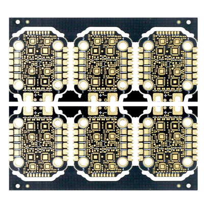
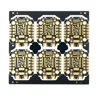
2oz 1.6mm Hdi Black PCB Board FR4 Quick PCB Prototype Immersion Au


Contact me for free samples and coupons.
Whatsapp:0086 18588475571
Wechat: 0086 18588475571
Skype: sales10@aixton.com
If you have any concern, we provide 24-hour online help.
xProduct Details
| PCB Name | Quick Pcb Prototype | Marterial | FR4, AntiCaf |
|---|---|---|---|
| Board Layer | 4L | Board Thickness | 1.6mm |
| Finished Copper Weight Outer | 2.0oz | Internal Copper Weight Inner | 2.0oz/70um |
| IPC Class Required | Class 3 | Smallest Hole Size | 0.2mm |
| Blind Vias | Yes | Application | Wifi Production |
| High Light | 2oz 1.6mm Black PCB Board,70um Black PCB Board,70um Quick PCB Prototype |
||
Product Description
2oz 1.6mm Hdi Black PCB Board FR4 Quick PCB Prototype Immersion Au
HDI PCB Board PCB Hdi Black PCB Board PCB Board Assembly Low Volume PCB Low Volume PCB Manufacture Quick PCB Prototype
4 Layer 1+N+1 HDI printed circuit board
| PCB Layer | HDI printed circuit board(4L) |
| PCB surface | Immersion Au 2u” |
| PCB material | FR-4, AntiCaf |
| PCB thickness | 1.6mm |
| Min. hole size | 0.20mm |
| PCB solder mask | Black, both side |
| PCB silkscreen | White, both sides |
| Finished Copper Weight Outer | 2.0oz |
| Internal Copper Weight Inner | 2.0oz/70um |
| IPC Class Required | Class 3 |
| Application | Wifi production |
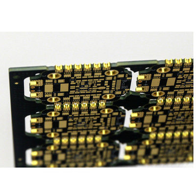
High-density interconnect (HDI) PCBs are characterized by finer lines, closer spaces, and more dense wiring. They have a faster connection while reducing the size of a project. Normally, these boards also feature blind and buried vias, laser ablated microvias, sequential lamination, and via in-pads. A HDI board can house the functionality of the previous boards used.
HDI Board Stack-up:
1+N+1 with laser microvia and mechanical buried core via. The “1” represents “build-up” or sequential lamination on each side of the core.
i+N+i (i>=2) PCBs contain 2 or more “build-up” of high-density interconnect layers. Microvias on different layers can be staggered or stacked. Copper filled stacked microvia structures are commonly seen in challenging designs.
![]()
![]()
FAQ:
1. What service can you provide?
PCB Manufacture,PCB Assembly,Rapid Prototype
2. How fast is your lead time?
Fastest 24H for 2L and 4L, 3WDs for HDI board.
3. How to get quick quotation?
Please provide gerber file and details of the board(including layer, board thickness, copper thickness, surface treatment, solder mask and silkscreen color, special request if any, demand quantity, etc)
sample:
| PCB Layer | 2L |
| PCB surface | LF-HASL |
| PCB material | FR4, TG170 |
| Copper thickness | 1/1oz finished |
| PCB solder mask | Double side,green |
| PCB silkscreen | Double side,White |
| Quantity | 15pcs,15 working day |
4.What payment terms do you have?
Wire Transfer(T/T)
Recommended Products