


All Products
Contact Person :
Yang
Phone Number :
18319054165
Whatsapp :
+8618319054165
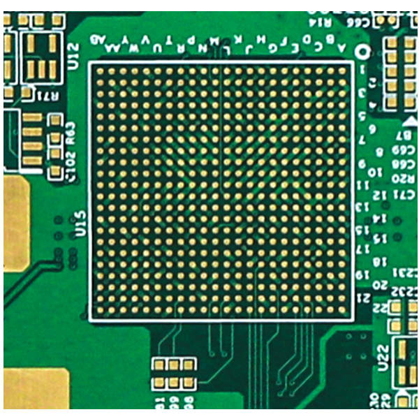
4 Layer HDI Printed Circuit Boards 1.6mm Green Solder Mask 3mil


Contact me for free samples and coupons.
Whatsapp:0086 18588475571
Wechat: 0086 18588475571
Skype: sales10@aixton.com
If you have any concern, we provide 24-hour online help.
xProduct Details
| PCB Name | 4L HDI Printed Circuit Boards | Marterial | FR-4, S1000-2 |
|---|---|---|---|
| Board Layer | 4L | Board Thickness | 1.6mm |
| Finished Copper Weight Outer | 1oz | Internal Copper Weight Inner | 1oz |
| Solder Mask | Green Solder Mask | Smallest Hole Size | 0.1mm |
| Blind/Burried Vias | Yes | Application | Telecommunication Product |
| High Light | 3mil HDI Printed Circuit Boards,4L HDI Printed Circuit Boards,3mil hdi pcb design |
||
Product Description
4 Layer HDI Printed Circuit Boards 1.6mm Green Solder Mask 3mil
HDI PCB Board 4 Layer Pcb Board HDI Printed Circuit Board HDI PCB Design PCB Manufacturing And Assembly
4L 1+N+1 HDI PCB
HDI PCB are abbreviation of high density interconnect printed circuit boards, they are characterized by finer lines, closer spaces, and more dense wiring.
For HDI boards own higher circuit density than traditional circuit boards, its designs can include smaller through holes and capture pads, and also higher connection pad density. They are widely used to reduce the weight and overall dimensions of products, as well as to enhance the electrical performance of the device.
HDI boards are applied to wide range of industries, like digital devices, smartphones and tablets, automobiles, aircraft and other vehicles products.
HDI Board Stack-up:
1+N+1 with laser microvia and mechanical buried core via. The “1” represents “build-up” or sequential lamination on each side of the core.
i+N+i (i>=2) PCBs contain 2 or more “build-up” of high-density interconnect layers. Microvias on different layers can be staggered or stacked. Copper filled stacked microvia structures are commonly seen in challenging designs.
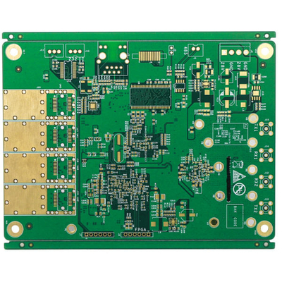
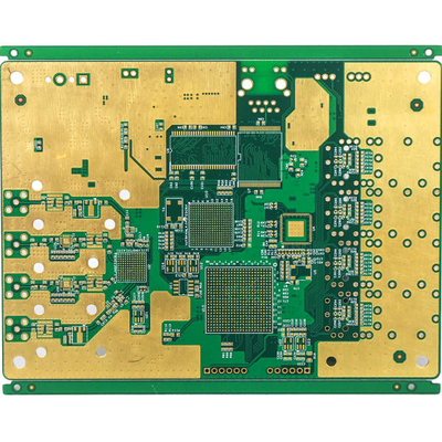
HSX products cover 1~32L FR-4 PCB, IMS PCB,HDI Boards, high frequency PTFE boards and Rigid-flex boards etc. It provides flexible quick turn production services (12 hours to72 hours), as well as small volume to big volume PCB manufacturing. Products are widely used in high-tech fields such as communications, power supplies, computer networks, digital products, industrial control, science and education, medical devices, and aerospace. HSX owns high-educated and experienced team and advanced production equipment.
| PCB Layer | 4L | PCB material | FR4 S1000-2 |
| Copper thickness | 1/1/1/1oz finished | PCB thickness | 1.6MM |
| Min. hole size | 0.1mm | Min.PCB track/gap: | 3mil |
| PCB solder mask | Green | PCB silkscreen | White |
| PCB surface finished | Immersion Gold 2u | PCB outline | Routing/V-CUT |
| Application | telecommunication product | ||
| Special requirement: | small line space and gap:3/3mil/HDI Buried vias and blind vias | ||
![]()
![]()
FAQ:
1. What service can you provide?
PCB Manufacture,PCB Assembly,Rapid Prototype
2. How fast is your lead time?
Fastest 24H for 2L and 4L, 3WDs for HDI board.
3. How to get quick quotation?
Please provide gerber file and details of the board(including layer, board thickness, copper thickness, surface treatment, solder mask and silkscreen color, special request if any, demand quantity, etc)
sample:
| PCB Layer | 6L |
| PCB surface | IMMERSION GOLD |
| PCB material | FR4, TG170 |
| Copper thickness | 3/3/3/3/3/3oz finished |
| PCB solder mask | Double side, Black |
| PCB silkscreen | Double side,White |
| Special requirement | Heavy copper 3OZ/small line space and gap:3/3mil |
4.What payment terms do you have?
Wire Transfer(T/T)
Recommended Products