


All Products
Contact Person :
Yang
Phone Number :
18319054165
Whatsapp :
+8618319054165
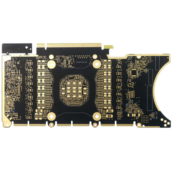
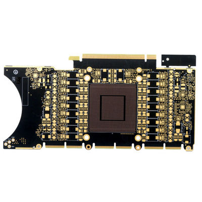
2oz Finished HDI PCB Board 2.0mm 6 Layer For Medical Devices


Contact me for free samples and coupons.
Whatsapp:0086 18588475571
Wechat: 0086 18588475571
Skype: sales10@aixton.com
If you have any concern, we provide 24-hour online help.
xProduct Details
| PCB Name | 6L 2+N+2 HDI PCB | Marterial | FR-4, TG170 |
|---|---|---|---|
| Board Layer | 6L | Board Thickness | 2.0mm |
| Finished Outer Copper Weight | 2oz Finished | Internal Copper Weight Inner | 2oz Base |
| Solder Mask | Black Solder Mask | Smallest Hole Size | 0.1mm |
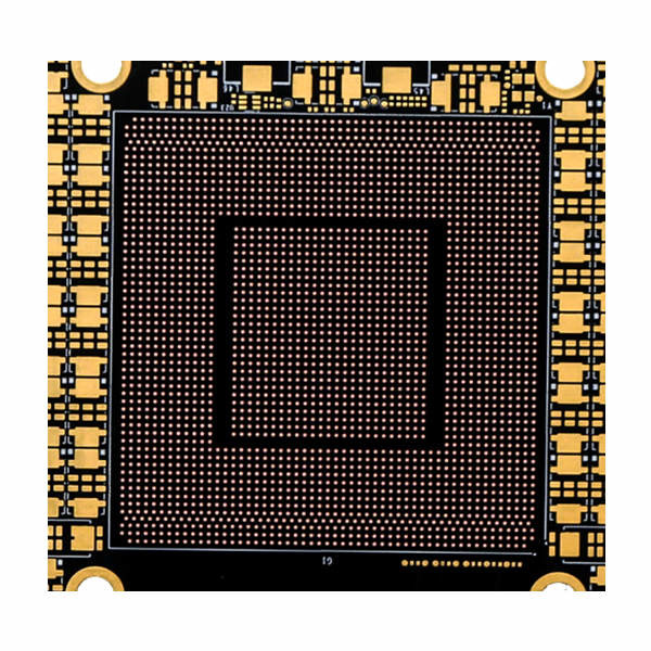
| Blind/Burried Vias | Yes, Requested | Application | Medical Devices Product |
| High Light | 2oz HDI PCB Board,2.0mm 2oz HDI PCB Board,2oz high density pcb |
||
Product Description
2oz Finished HDI PCB Board 2.0mm 6 Layer For Medical Devices
HDI PCB Board Printed Circuit Board Assembly Companies Contract Manufacturing PCB Assembly
4L 2+N+2 HDI PCB
High density interconnect printed circuit boards are also called HDI boards, being characterized by finer lines, closer spaces, and more dense wiring. its designs can include smaller through holes and capture pads, and also higher connection pad density. They are widely used to reduce the weight and overall dimensions of products, as well as to enhance the electrical performance of the device.
Application: digital devices products, smartphones and tablets products, automobiles and telecomunication products, aircraft and other vehicles products, etc.
Normal Stack-up:
1+N+1 with laser microvia and mechanical buried core via. The “1” represents “build-up” or sequential lamination on each side of the core.
i+N+i (i>=2) PCBs contain 2 or more “build-up” of high-density interconnect layers. Microvias on different layers can be staggered or stacked. Copper filled stacked microvia structures are commonly seen in challenging designs.
HSX products cover 1~32L FR-4 PCB, IMS PCB,HDI Boards, high frequency PTFE boards and Rigid-flex boards etc. It provides flexible quick turn production services (12 hours to72 hours), as well as small volume to big volume PCB manufacturing. Products are widely used in high-tech fields such as communications, power supplies, computer networks, digital products, industrial control, science and education, medical devices, and aerospace. HSX owns high-educated and experienced team and advanced production equipment.
| PCB Layer | 6L 2+N+2 | PCB material | FR4 TG170 |
| Copper thickness | 2/2/2/2/2/2oz finished | PCB thickness | 2.0MM |
| Min. hole size | 0.1mm | Min.PCB track/gap: | 3.5mil |
| PCB solder mask | Green | PCB silkscreen | White |
| PCB surface finished | ENIG 2u | PCB outline | Routing/V-CUT |
| Application | Medical devices product | ||
| Special requirement: | HDI Buried vias and blind vias,two step stack up | ||
![]()
![]()
FAQ:
Q1:Are you a factory or trade company?
A: Yes, we are the factory, we have independent quick turn prototype PCB manufacturing & big volume PCB production lines.
Q2:What kind of PCB file format can you accept for production?
A: Gerber, PROTEL 99SE, PROTEL DXP, POWER PCB, CAM350, ODB+(.TGZ)
Q3:Are my PCB files safe when I submit them to you for manufacturing?
A: We respect customer's copyright and will never manufacture PCB for someone else with your files unless we receive written permission from your side, nor we'll share these files with any other 3rd parties. And we could sign NDA with client if necessary.
Q4:If we have no PCB file/Gerber file, only have the PCB sample,can you produce it for me?
A: Yes,we could help you to clone the PCB. Just send the sample PCB to us, we could clone the PCB design and work out it.
Q5:What is your standard lead time for PCB?
A: Sample/prototype(less than 3sqm):
1-2 Layers: 3 to 5working days (fastest 24hours for quick turn services)
4-8 Layers: 7~12 working days (fastest 48hours for quick turn services)
Mass production (less than 200sqm):
1-2 Layers:7 to 12 working days
4-8 Layers:10 to 15 working days
Q6:What payment do you accept ?
A: Wire Transfer(T/T) or Letter of Credit(L/C) or Paypal(only for small value less than 500usd)
Q7:How will you usually ship the PCB?
A: Usually for small packages, we will ship the boards by DHL,UPS,FedEx door to door service, we could use your shipping account to do collection or use our account to ship in DDU (import duty unpaid) delivery term.
For heavy goods more than 300kg, we may ship your PCB boards by ship or by air to save freight cost. Of course, if you have your own forwarder, we may contact them for dealing with your shipment.
Recommended Products