


All Products
Contact Person :
Yang
Phone Number :
18319054165
Whatsapp :
+8618319054165
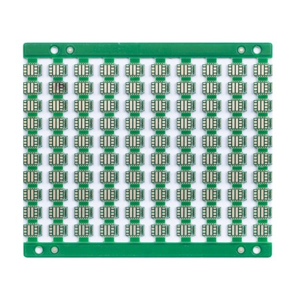
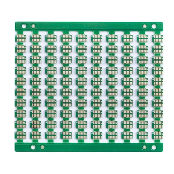
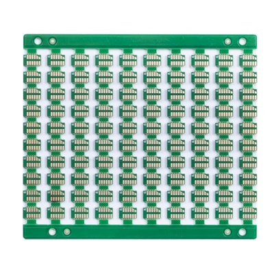
1.6mm High Density Pcb 4mil Electronic Circuit Board FR4 TG170


Contact me for free samples and coupons.
Whatsapp:0086 18588475571
Wechat: 0086 18588475571
Skype: sales10@aixton.com
If you have any concern, we provide 24-hour online help.
xProduct Details
| PCB Name | Electronic Circuit Board | Marterial | FR4 TG170 |
|---|---|---|---|
| Board Layer | 4L | Board Thickness | 1.6mm |
| Copper Thickness | 1/1/1/1OZ Finished | Min.PCB Track/gap | 4/4mil |
| Solder Mask | Green, 2 Sides | Smallest Mechanical Drilling Hole | 0.2mm |
| Special Request | Impedance Control/resin Filled And Plated Over | Applicationcommunications Products | Digital Products |
| High Light | 1.6mm High Density Pcb,4mil High Density Pcb,4mil Electronic Circuit Board |
||
Product Description
1.6mm High Density Pcb 4mil Electronic Circuit Board FR4 TG170
HDI PCB Board Electronic Pcb Board Printed Circuit Board Assembly Services Printed Circuit Board Assembly
4L 1+N+1 HDI Boards
HDI PCB means high density interconnect printed circuit boards, they are characterized by finer lines, closer spaces, and more dense wiring.
Due to its higher circuit density than traditional circuit boards, HDI PCB designs can include smaller through holes and capture pads, as well as higher connection pad density. HDI PCB is widely used to reduce the weight and overall dimensions of products, as well as to enhance the electrical performance of the device.
HDI Board Stack-up:
1+N+1 with laser microvia and mechanical buried core via. The “1” represents “build-up” or sequential lamination on each side of the core.
i+N+i (i>=2) PCBs contain 2 or more “build-up” of high-density interconnect layers. Microvias on different layers can be staggered or stacked. Copper filled stacked microvia structures are commonly seen in challenging designs.
HSX products cover 1~32L FR-4 PCB, IMS PCB,HDI Boards, high frequency PTFE boards and Rigid-flex boards etc. It provides flexible quick turn production services (12 hours to72 hours), as well as small volume to big volume PCB manufacturing.Products are widely used in high-tech fields such as communications, power supplies, computer networks, digital products, industrial control, science and education, medical devices, and aerospace.
| Circuit board Layer count: | 4L | Circuit board laminate: | FR4 TG170 |
| Layer Copper thick: | 1/1/1/1OZ | Board thickness: | 0.8MM |
| Smallest hole size: | 0.20mm | Smallest PCB track/gap: | 4/4mil |
| Solder mask color: | Green | Silk screen color: | White |
| PCB surface finished: | Immersion Gold | Board profile: | Routing |
| PCB Board Application: | digital products | ||
| Requesting Special requirement: | impedance control/resin filled and plated over/big au area | ||
![]()
![]()
FAQ:
Q1:What services could you provide?
A: PCB Manufacture,PCB Assembly,Rapid Prototype order, and so on
Q2:If we have no PCB file/Gerber file, only have the PCB sample,can you produce it for me?
A: Yes,we could help you to clone the PCB. Just send the sample PCB to us, we could clone the PCB design and work out it.
Q3:What is your standard lead time for PCB?
A: Sample/prototype(less than 3sqm):
1-2 Layers: 3 to 5working days (fastest 24hours for quick turn services)
4-8 Layers: 7~12 working days (fastest 48hours for quick turn services)
Mass production (less than 200sqm):
1-2 Layers:7 to 12 working days
4-8 Layers:10 to 15 working days
Q4: Does our product will be tested before shipment.
A: Yes. We could provide Function Circuit Testing if you provide us the testing methods.
Q5:How to get quick quotation?
A: Please provide gerber file and details of the board(including layer, board thickness, copper thickness, surface treatment, solder mask and silkscreen color, special request if any, demand quantity, etc)
sample:
PCB Layer: 2L/4L/6L/8L/10L/12L
PCB material/Base material: FR4, TG170; FR, SHENGYI/FR4,IT180A; Rogers+FR4 TG170; FR4+PI
Copper thickness: 1/1oz finished; 2/2oz finished; 1/1/1/1oz finished; 2/2/2/2oz finished; 1oz inner base and 1oz outer finished;
PCB solder mask/ Solder mask Color: Green for both sides; Blue for both sides; Black for both sides; White for both sides
PCB silkscreen: Double side,White; N/A; Black for both sides
Quantity: 15pcs, 5 working day; 1000pcs, 14 working days;
Recommended Products