


All Products
Contact Person :
Yang
Phone Number :
18319054165
Whatsapp :
+8618319054165
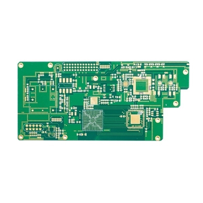
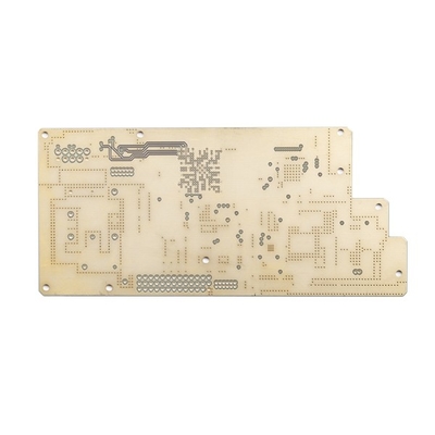
FR4 BGA Quick Turn PCB Boards 6 Layer 8mil Green Solder Mask Big Au Area


Contact me for free samples and coupons.
Whatsapp:0086 18588475571
Wechat: 0086 18588475571
Skype: sales10@aixton.com
If you have any concern, we provide 24-hour online help.
xProduct Details
| PCB Name | 6 Layer Quick Turn PCB With Large Au Area | Marterial | FR4 |
|---|---|---|---|
| Surface Finished | Immersion Gold, Gold Finger | Board Thickness | 1.6MM |
| Copper Thickness | 1/1/1/1/1/1OZ | Min. Line Distance/space | 8/8mil |
| Solder Mask | Green Solder Mask | Smallest Mechanical Drilling Hole | 0.3mm |
| Special Requirement | Impedance Control/0.25mm BGA/big Au Area | Applicationcommunications Products | Digital Product |
| High Light | 8mil Quick Turn PCB Boards,BGA Quick Turn PCB Boards,8mil bga pcb board |
||
Product Description
FR4 BGA Quick Turn PCB Boards 6 Layer 8mil Green Solder Mask Big Au Area
Quick Turn PCB Boards Digital Product Big Au Area Little BGA FAST Massive Volume Order Fast Sample Order
6 Layer Quick Turn PCB with Large Au Area
H SX Circuit’s Advantages:
1)Professional manufacturing PCB for 10 years
2) High-end positioning, professional production line
3) Stable and mature manufacturing technology
4) High reliability quality assurance
5) Comprehensive market service system
6) Quick response, fast delivery
Min finish panel size is 5 * 5mm
PCB material includes PI +FR4,FR4, Rogers, etch
PCB thickness capability is 0.2~4.0mm(needs to review when <0.2 mm, or >4 mm ) (and can not do HASL surface with board thickness </=0.6mm)
Copper thickness of inner and outer base copper capability: Min 0.3/0.5oz,Max 3oz, advance 4-6oz
Bow and twist tolerance: 0.075%
Min. hole size: 0.15mm(need to review the board if smaller than 0.15 mm )
HDI Min drill hole capability: 0.08-0.10MM
PCB track/gap capability: 3mil(0.075mm)
PCB outline method: Routing/V-CUT/Punching
Solder mask thickness capability: standard 15-20um; Advanced: 35um
Min solder mask bridge width capability: green 4mil,other colour 4.8mil
Solder mask filling holes capability: 0.1-0.5mm
The color of solder mask covers green, matt green, blue, matt blue, black, matt black, yellow, red, white, etc
PCB silkscreen includes white, Black and as your request
Peelable mask thickness capability: 500-1000um
Oxidation film of OSP capability: 0.2-0.5um
| Layer counts: | 6 layer | Circuit board laminate: | FR4 |
| Different Copper thickness: | 1/1/1/1/1/1OZ | PCB Board thick: | 1.0 MM |
| Smallest Mechanical drilling hole: | 0.30 mm | Min. line distance/space: | 8/8mil |
| Solder mask color: | Green | Legends' color: | White |
| PCB surface finished: | Immersion Gold | Board profile: | Milling |
| PCB Board Application: | digital products | ||
| Requesting Special requirement: | impedance control/0.25mm BGA/big au area | ||
![]()
FAQ:
Q1:Could you provide PCB Assembly services and components sourcing?
A: Yes, we could also provide components sourcing and PCB Assembly services as well as box build if request.
Q2:Which countries have you worked with?
A:USA, Canada, Italy, Germany, UK, Spain, France, Russia, Iran, Turkey, Czech Republic,Austria, Australia, Brazil, Japan, India etc.
Q3:Are my PCB files safe when I submit them to you for manufacturing?
A: We respect customer's copyright and will never manufacture PCB for someone else with your files unless we receive written permission from your side, nor we'll share these files with any other 3rd parties. And we could sign NDA with client if necessary.
Q4:If we have no PCB file/Gerber file, only have the PCB sample,can you produce it for me?
A: Yes,we could help you to clone the PCB. Just send the sample PCB to us, we could clone the PCB design and work out it.
Q5:What is your standard lead time for PCB?
A: Sample/prototype(less than 3sqm):
1-2 Layers: 3 to 5working days (fastest 24hours for quick turn services)
4-8 Layers: 7~12 working days (fastest 48hours for quick turn services)
Mass production (less than 200sqm):
1-2 Layers:7 to 12 working days
4-8 Layers:10 to 15 working days
Recommended Products