


All Products
Contact Person :
Yang
Phone Number :
18319054165
Whatsapp :
+8618319054165
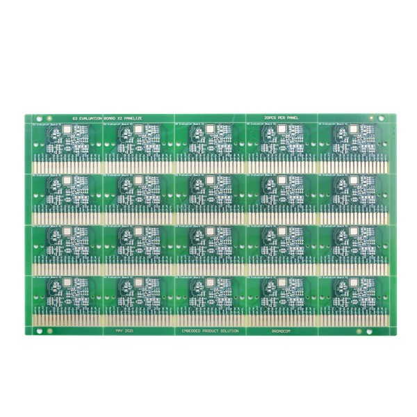
Resin Plugged Hole Multilayer Circuit Board ENIG Surface 4L Halogen Free 1.6mm


Contact me for free samples and coupons.
Whatsapp:0086 18588475571
Wechat: 0086 18588475571
Skype: sales10@aixton.com
If you have any concern, we provide 24-hour online help.
xProduct Details
| Product Name | 4L Halogen Free Resin Filled PCB | Material | FR4 Halogen Free |
|---|---|---|---|
| Finished Treatment | ENIG 2u | Board Thickness | 1.6mm |
| Finished Copper Thickness | 1/1/1/1OZ | 6L Halogen Free Printed Circuit Board | 0.2mm |
| Min.PCB Track/gap | 8/8mil | Solder Mask Color | Green |
| Silkscreen Color | White | Special Request | Impedance Control/resin Filled And Plated Over |
| High Light | 4L Multilayer Circuit Board,1.6mm Multilayer Circuit Board,1.6mm multilayer board |
||
Product Description
Resin Plugged Hole Multilayer Circuit Board ENIG Surface 4L Halogen Free 1.6mm
Multilayer Printed Circuit Board Resin Plugged Hole And Plated Over PCB ENIG Surface Impedance Control PCB
4L Halogen Free Resin filled PCB
Max layers: 32layer (≥20 layer needs to review)
Max finish panel size: 740* 500 MM(>600 MM needs to review)
Min finish panel size: 5 * 5mm
Min drill hole: 0.15mm(<0.15 mm needs to review)
HDI Min drill hole: 0.08-0.10MM
Aspect ratio: 15:1 (>12:1 needs to review)
Board thickness: 0.2~4.0mm(<0.2 mm,>4 mm needs to review)
Copper thickness: Inner layer≤ 6 OZ(≥5 OZ for 4L,≥4OZ for 6L,≥3OZfor 8L and above shall be reviewed)
Outer layer copper≤ 10 OZ(≥5 OZ needs to review)
Copper in holes≤ 5 OZ(≥1 OZ needs to review
Min space in inner layer(one-sided): 4~8L(include): sample: 4 mil; small volume: 4.5 mil;
8~12L(include): sample: 5 mil; small volume: 5.5 mil
12~18L(include): sample: 6 mil; small volume: 6.5 mil
|
||||||||||||||||||||||||||||
![]()
FAQ:
Q1:Are you a factory or trade company?
A: Yes, we are the factory, we have independent quick turn prototype PCB manufacturing & big volume PCB production lines.
Q2:What kind of PCB file format can you accept for production?
A: Gerber, PROTEL 99SE, PROTEL DXP, POWER PCB, CAM350, ODB+(.TGZ)
Q3:Are my PCB files safe when I submit them to you for manufacturing?
A: We respect customer's copyright and will never manufacture PCB for someone else with your files unless we receive written permission from your side, nor we'll share these files with any other 3rd parties. And we could sign NDA with client if necessary.
Q4:If we have no PCB file/Gerber file, only have the PCB sample,can you produce it for me?
A: Yes,we could help you to clone the PCB. Just send the sample PCB to us, we could clone the PCB design and work out it.
Q5:What is your standard lead time for PCB?
A: Sample/prototype(less than 3sqm):
1-2 Layers: 3 to 5working days (fastest 24hours for quick turn services)
4-8 Layers: 7~12 working days (fastest 48hours for quick turn services)
Mass production (less than 200sqm):
1-2 Layers:7 to 12 working days
4-8 Layers:10 to 15 working days
Q6:What payment do you accept ?
A: Wire Transfer(T/T) or Letter of Credit(L/C) or Paypal(only for small value less than 500usd)
Recommended Products