


All Products
Contact Person :
Yang
Phone Number :
18319054165
Whatsapp :
+8618319054165
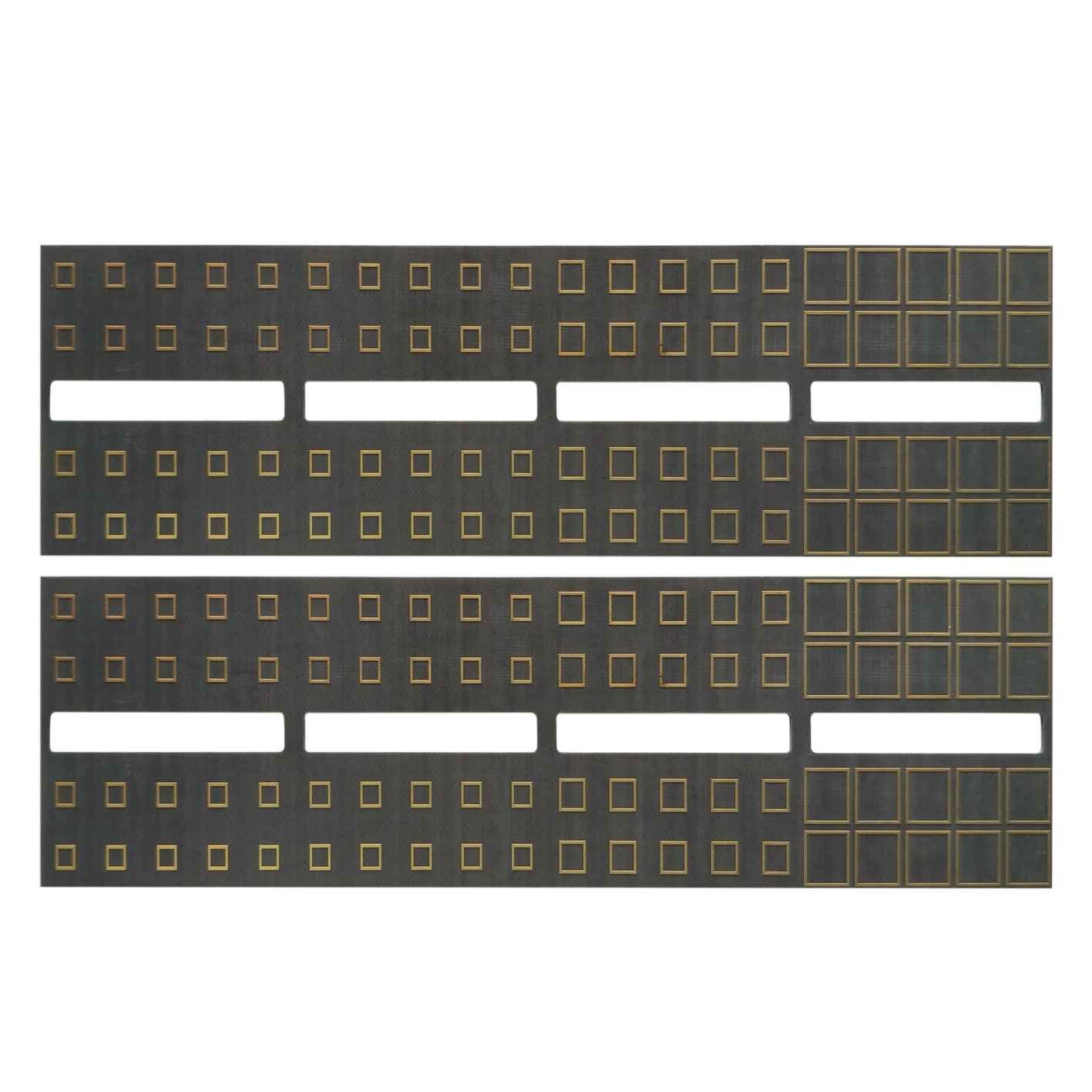
Black Solder Mask Taconic PCB 2.0mm High Speed Circuit Design 2oz

Contact me for free samples and coupons.
Whatsapp:0086 18588475571
Wechat: 0086 18588475571
Skype: sales10@aixton.com
If you have any concern, we provide 24-hour online help.
xProduct Details
| PCB Name | High Frequency Printed Circuit Board | Marterial | Rogers FR4 |
|---|---|---|---|
| Surface Finished | Immersion Gold | Board Thickness | 2.0mm |
| Copper Thickness | 1/1 OZ | Solder Mask | Black |
| High Light | 2.0mm Taconic PCB,2oz Taconic PCB,2oz High Speed Circuit Design |
||
Product Description
Black Solder Mask Taconic PCB 2.0mm High Speed Circuit Design 2oz
High Frequency PCB High Frequency Printed Circuit Board Black Solder Mask Taconic PCB ROHS Compliant PCB
High Frequency Printed Circuit Board
A high frequency printed circuit board, whether it’s rigid or flex, offers faster signal flow rates and a frequency range of up to 100 GHz. It’s important to note that there are numerous materials designed to operate at high frequency levels. HF PCBs are defined by lower dielectric constant (Dk), lower dissipation factor (Df), and low levels of thermal expansion. They are used regularly for HDI technology. They are also used extensively in high speed communications, telecommunications, and RF microwave technology.
Depending on the parameters, the HF signal is reflected on the circuit board, which means that the impedance (dynamic resistance) changes relative to the transmitting component. To avoid such capacitive effects, all parameters must be specified accurately and implemented with the highest level of process control.
High frequency printed circuit boardis are widely used for special signal transmission between objects. It operates from 500MHz to 2GHz and is right for mobile, microwave, RF and high-speed design applications. With the increasing complexity of electronic components and switches, faster signal flow and better transmission frequency are needed. High frequency PCB can play a really important role.Due to the short rise time of the pulse in electronic components, it is necessary to consider the conductor width as an electronic component in HF technology.
| Feature | Capability |
| Quality Grade | Standard IPC 2 |
| Number of Layers | 2- 24layers |
| Material | ROGERS, TACONIC, ARLON, FR4, |
| Board Size | Min 5mm x 5mm | Max 500mm x 745mm |
| Board Thickness | 0.2mm - 4.0mm |
| Copper Weight(Finished) | 0.5oz - 2oz |
| Min Tracing/Spacing | 3mil/3mil |
| Solder Mask Color | Green, White, Blue, Black, Red, Yellow... |
| Silkscreen Color | White, Black, Yellow... |
| Surface Finish | Electroless nickel/immersion gold (ENIG) - RoHS |
| Immersion silver - RoHS | |
| Immersion tin - RoHS | |
| Min Annular Ring | 0.1mm |
| Min Drilling Hole Diameter | 0.15mm |
| Other Techniques | Peelable solder mask |
| Gold fingers | |
| Carbon oil | |
| Countersink holes |
![]()
![]()
FAQ:
Q1:Could you provide PCB Assembly services and components sourcing?
A: Yes, we could also provide components sourcing and PCB Assembly services as well as box build if request.
Q2:Which countries have you worked with?
A:USA, Canada, Italy, Germany, UK, Spain, France, Russia, Iran, Turkey, Czech Republic,Austria, Australia, Brazil, Japan, India etc.
Q3:Are my PCB files safe when I submit them to you for manufacturing?
A: We respect customer's copyright and will never manufacture PCB for someone else with your files unless we receive written permission from your side, nor we'll share these files with any other 3rd parties. And we could sign NDA with client if necessary.
Q4:If we have no PCB file/Gerber file, only have the PCB sample,can you produce it for me?
A: Yes,we could help you to clone the PCB. Just send the sample PCB to us, we could clone the PCB design and work out it.
Q5:What is your standard lead time for PCB?
A: Sample/prototype(less than 3sqm):
1-2 Layers: 3 to 5working days (fastest 24hours for quick turn services)
4-8 Layers: 7~12 working days (fastest 48hours for quick turn services)
Mass production (less than 200sqm):
1-2 Layers:7 to 12 working days
4-8 Layers:10 to 15 working days
Recommended Products