


All Products
Contact Person :
Yang
Phone Number :
18319054165
Whatsapp :
+8618319054165
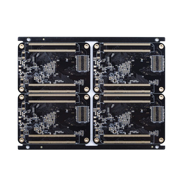
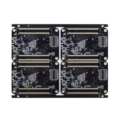
8 Layer Multilayer Printed Circuit Board ENIG 2u TAIYO Black Solder Mask

Contact me for free samples and coupons.
Whatsapp:0086 18588475571
Wechat: 0086 18588475571
Skype: sales10@aixton.com
If you have any concern, we provide 24-hour online help.
xProduct Details
| PCB Layer | 8 Layer Printed Circuit Board With Small Line Space And BGA | Marterial | FR4 TG170 |
|---|---|---|---|
| PCB Surface | ENIG 2u | Solder Mask | TAIYO Black |
| Smallest PCB Track/gap | 3/3mil | Smallest Hole | 0.20mm |
| Application | Digital Products | Lead Time | Fastest 24H For 2L And 4L |
| Highlight | 8 Layer Multilayer Printed Circuit Board,TAIYO Black Multilayer Printed Circuit Board,ENIG 8 Layer Printed Circuit Board |
||
Product Description
Multilayer Printed Circuit Board 8 Layer Printed Circuit Board With Small Line Space And BGA Black Solder Mask
8 Layer Printed Circuit Board with Small line space and BGA
HSX Circuit covers over 5,000 PCB products monthly, from single layer to 32L FR-4 PCB, from IMS PCB,HDI Boards, to high frequency PTFE boards and Rigid-flex boards. We provides flexible quick turn production services (12 hours to72 hours), as well as small volume to big volume PCB manufacturing.
Products are widely used in high-tech fields such as communications, power supplies, computer networks, digital products, industrial control, science and education, medical devices, and aerospace.
Max layers: 32layer (≥20 layer needs to review)
Max finish panel size: 740* 500 MM(>600 MM needs to review)
Min finish panel size: 5 * 5mm
PCB material: PI +FR4,FR4, Rogers...
PCB thickness: 0.2~4.0mm(<0.2 mm,>4 mm needs to review) (Board thickness ≤ 0.6mm,do not apply for HASL surface)
copper thickness of inner and outer base copper: Min 0.3/0.5oz,Max 3oz, advance 4-6oz
Bow and twist: 0.075%
Min. hole size: 0.15mm(<0.15 mm needs to review)
HDI Min drill hole: 0.08-0.10MM
PCB track/gap: 3mil(0.075mm)
PCB outline: Routing/V-CUT/Punching
Solder mask thickness: standard 15-20um; Advanced: 35um
Min solder mask bridge width: green 4mil,other colour 4.8mil
Solder mask filling holes: 0.1-0.5mm
The color of solder mask: green,matt green,blue,matt blue,black,matt black,yellow,red,white,etc
PCB silkscreen: White, Black and as your request
Peelable mask thickness: 500-1000um
Oxidation film of OSP: 0.2-0.5um
| Circuit board Layer count: | 8L | Circuit board laminate: | FR4 TG170 |
| Layer Copper thick: | 1/1/1/1/1/1/1/1OZ | Board thickness: | 1.6MM |
| Smallest hole size: | 0.2mm | Smallest PCB track/gap: | 3/3mil |
| Solder mask color: | TAIYO Black | Silk screen color: | White |
| PCB surface finished: | Immersion Gold | Board profile: | Routing/V-CUT |
| PCB Board Application: | digital products | ||
| Requesting Special requirement: | small line space and gap:3/3mil/impedance control/resin filled and plated over/0.25mm BGA | ||
![]()
![]()
FAQ:
Q1:Are you a factory or trade company?
A: Yes, we are the factory, we have independent quick turn prototype PCB manufacturing & big volume PCB production lines.
Q2:What kind of PCB file format can you accept for production?
A: Gerber, PROTEL 99SE, PROTEL DXP, POWER PCB, CAM350, ODB+(.TGZ)
Q3:Are my PCB files safe when I submit them to you for manufacturing?
A: We respect customer's copyright and will never manufacture PCB for someone else with your files unless we receive written permission from your side, nor we'll share these files with any other 3rd parties. And we could sign NDA with client if necessary.
Q4:If we have no PCB file/Gerber file, only have the PCB sample,can you produce it for me?
A: Yes,we could help you to clone the PCB. Just send the sample PCB to us, we could clone the PCB design and work out it.
Q5:What is your standard lead time for PCB?
A: Sample/prototype(less than 3sqm):
1-2 Layers: 3 to 5working days (fastest 24hours for quick turn services)
4-8 Layers: 7~12 working days (fastest 48hours for quick turn services)
Mass production (less than 200sqm):
1-2 Layers:7 to 12 working days
4-8 Layers:10 to 15 working days
Q6:What payment do you accept ?
A: Wire Transfer(T/T) or Letter of Credit(L/C) or Paypal(only for small value less than 500usd)
Recommended Products