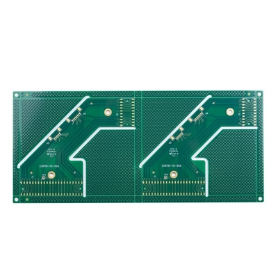
10L Multilayer Printed Circuit Board Impedance Control Immersion Gold ENIG

Contact me for free samples and coupons.
Whatsapp:0086 18588475571
Wechat: 0086 18588475571
Skype: sales10@aixton.com
If you have any concern, we provide 24-hour online help.
x| PCB Layer | 10L Printed Circuit Board ENIG | Marterial | FR4, TG170 |
|---|---|---|---|
| PCB Surface | Immersion Gold/ENIG | Solder Mask | Green |
| Smallest PCB Track/gap | 4/4mil | Smallest Hole | 0.2mm |
| ApplicationIndustrial Control Products | Industrial Control | Special Requirement | Copper Filled Via/Impedance Control/Press-fit Hole |
| High Light | 10L Multilayer Printed Circuit Board,4/4mil Multilayer Printed Circuit Board,ENIG Printed Circuit Board |
||
Multilayer Printed Circuit Board 10L PCB Impedance Control Immersion Gold ENIG Electronic Circuit Board
10L Printed Circuit Board ENIG
HSX products cover 1~32L FR-4 PCB, IMS PCB,HDI Boards, high frequency PTFE boards and Rigid-flex boards etc. It provides flexible quick turn production services (12 hours to72 hours), as well as small volume to big volume PCB manufacturing.Products are widely used in high-tech fields such as communications, power supplies, computer networks, digital products, industrial control, science and education, medical devices, and aerospace.
Max layers: 32layer (≥20 layer needs to review)
Max finish panel size: 740* 500 MM(>600 MM needs to review)
Min finish panel size: 5 * 5mm
PCB material: PI +FR4,FR4, Rogers
PCB thickness: 0.2~4.0mm(<0.2 mm,>4 mm needs to review) (Board thickness ≤ 0.6mm,do not apply for HASL surface)
Copper thickness of inner and outer base copper: Min 0.3/0.5oz,Max 3oz, advance 4-6oz
Bow and twist: 0.075%
Min. hole size: 0.15mm(<0.15 mm needs to review)
HDI Min drill hole: 0.08-0.10MM
PCB track/gap: 3mil(0.075mm)
PCB outline: Routing/V-CUT/Punching
Solder mask thickness: standard 15-20um; Advanced: 35um
Min solder mask bridge width: green 4mil,other colour 4.8mil
Solder mask filling holes: 0.1-0.5mm
The color of solder mask: green,matt green,blue,matt blue,black,matt black,yellow,red,white,etc
PCB silkscreen: White, Black and as your request
Peelable mask thickness: 500-1000um
Oxidation film of OSP: 0.2-0.5um
| Circuit board Layer count: | 10L | Circuit board Raw Material: | FR4 TG170 IT180A |
| Layer Copper thick: | 1/1/1/1/1/1/1/1OZ | Board thickness: | 1.6MM |
| Smallest hole size: | 0.2mm | Smallest PCB track/gap: | 4/4mil |
| Solder mask color: | Green | Silk screen color: | White |
| PCB surface finished: |
Immersion Gold/ENIG |
Board profile: | Routing & Routing |
| PCB Board Application: | Industrial Control | ||
| Requesting Special requirement: | Copper Filled Via/Impedance Control/Press-fit Hole | ||
![]()
![]()
FAQ:
Q1:What kind of PCB file format can you accept for production?
A: Gerber, PROTEL 99SE, PROTEL DXP, POWER PCB, CAM350, ODB+(.TGZ)
Q2. What any other information should be offered except for file?
A: Following specifications are needed for quotation:
1) Base material
2) Board thickness:
3) Copper thickness
4) Surface treatment:
5) color of solder mask and silkscreen
6) Quantity
Q3. No PCB file/GBR file, only have the PCB sample, can you produce it for me?
A: Yes, we could help you to clone the PCB. Just send the sample PCB to us, we could clone the PCB design and work out it.
Q4. What’s the BOM?
A: BOM is a Bill of Materials that list the components required to build your project. BOM’s include part number, brand, reference designator , quantity, and description of parts that need to be assembled.
Q5. Where are your circuit boards manufactured?
A: As a China-based professional PCB manufacturer, all circuit boards are manufactured in China.


