


All Products
Contact Person :
Yang
Phone Number :
18319054165
Whatsapp :
+8618319054165
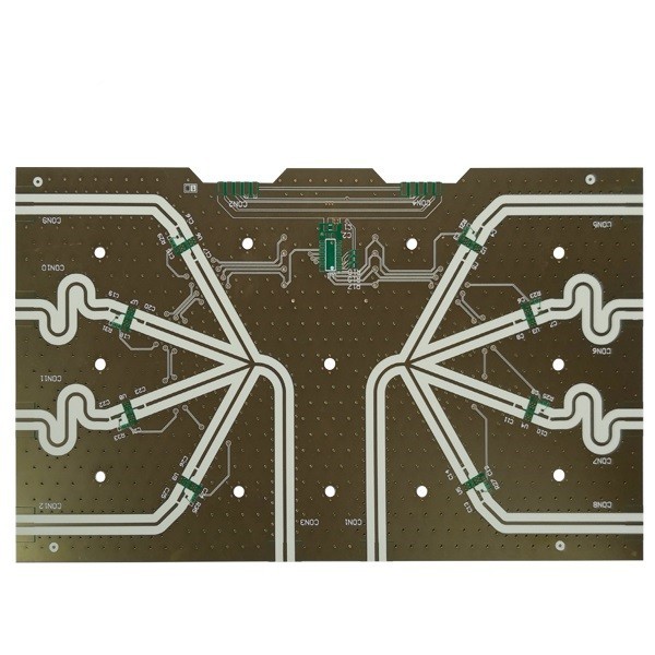
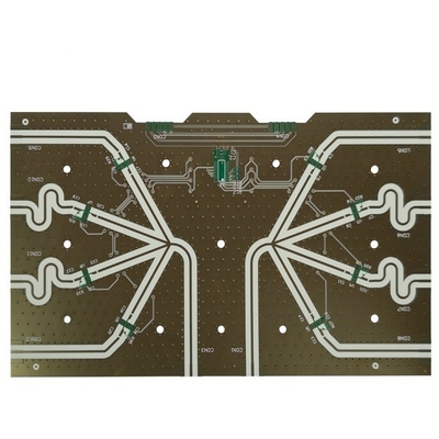
Immersion Gold High Density Interconnect Pcb Board 6 Layer FR4 TG170

Contact me for free samples and coupons.
Whatsapp:0086 18588475571
Wechat: 0086 18588475571
Skype: sales10@aixton.com
If you have any concern, we provide 24-hour online help.
xProduct Details
| PCB Name | High Density Interconnect Pcb | Marterial | FR4 TG170 |
|---|---|---|---|
| Board Layer | 6L | Board Thickness | 0.8mm |
| Min.PCB Track/gap | 4/3mil | Solder Mask | Blue |
| Smallest Mechanical Drilling Hole | 0.15mm | Special Request | Min. Via Hole Size 0.15mm/impedance Control/half Hole |
| High Light | TG170 High Density Interconnect Pcb,6L High Density Interconnect Pcb,Immersion Gold hdi rigid flex pcb |
||
Product Description
Immersion Gold High Density Interconnect Pcb Board 6 Layer FR4 TG170
6L 1+N+1 HDI Boards
What’s HDI PCB? High-density interconnect (HDI) PCBs are characterized by finer lines, closer spaces, and more dense wiring, which allow for a faster connection while reducing the size and bulk of a project. These boards also feature blind and buried vias, laser ablated microvias, sequential lamination, and via in-pads.
A HDI board can house the functionality of the previous boards used. MADPCB is an HDI PCB manufacturer and provider in Shenzhen, China supports HDI PCB prototype and mass production with less expensive price and quick-turn lead time. Customers from a variety of industries we serve have a common that have high expectations in quality, reliability and on-time delivery in HDI PCB production. Our quality is not afterthought, but built into each process from front-end to fabrication and shipping.
| PCB Layer | 6L | PCB material | FR4 TG170 |
| Copper thickness | 1/1/1/1/1/1OZ | PCB thickness | 0.80MM |
| Min. hole size | 0.15mm | Min.PCB track/gap: | 4/3mil |
| PCB solder mask | Blue | PCB silkscreen | White |
| PCB surface finished | Immersion Gold | PCB outline | Routing |
| Application | digital products | ||
| Special requirement: | small line space and gap:4/3mil/HDI Buried vias and blind vias, one step stack up /min. via hole size 0.15mm/impedance control/half hole/0.25mm BGA/plating edge | ||
Application of PCB Printed Circuit Board:
1, Telecom Communication
2, Consumer Electronics
3, Security monitor
4, Vehicle Electronices
5, Smart Home
6, Industrial controls
7, Military & Defense
![]()
![]()
Advantage Of PCB Printed Circuit Board
• Strict product liability, taking IPC-A-160 standard
• Engineering pretreatment before production
• Production process control (5Ms)
• 100% E-test, 100% visual inspection, including IQC, IPQC, FQC, OQC
• 100% AOI inspection, including X-ray, 3D microscope and ICT
• High-voltage test, impedance control test
• Micro section, soldering capacity, thermal stress test, shocking test
Recommended Products